- 您现在的位置:买卖IC网 > Sheet目录1998 > ICS844021BG-01LFT (IDT, Integrated Device Technology Inc)IC CLOCK GEN ETHERNET 8-TSSOP
IDT / ICS LVDS CLOCK GENERATOR
7
ICS844021BG-01 REV. A OCTOBER 23, 2012
ICS844021-01
FEMTOCLOCKS CRYSTAL-TO-LVDS CLOCK GENERATOR
APPLICATION INFORMATION
FIGURE 2. CRYSTAL INPUt INTERFACE
CRYSTAL INPUT INTERFACE
The ICS844021-01 has been characterized with 18pF parallel
resonant crystals. The capacitor values, C1 and C2, shown in
Figure 2 below were determined using a 25MHz, 18pF parallel
resonant crystal and were chosen to minimize the ppm error.
The optimum C1 and C2 values can be slightly adjusted for
different board layouts.
C1
33p
X1
18pF Parallel Crystal
C2
27p
XTAL_OUT
XTAL_IN
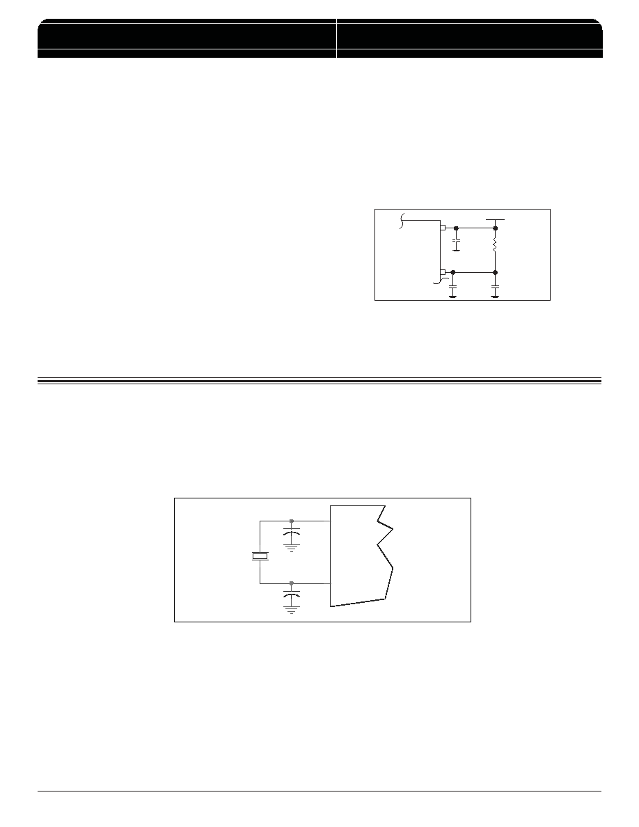
POWER SUPPLY FILTERING TECHNIQUES
As in any high speed analog circuitry, the power supply pins are
vulnerable to random noise. To achieve optimum jitter perfor-
mance, power supply isolation is required. The ICS844021-01
provides separate power supplies to isolate any high switching
noise from the outputs to the internal PLL. V
DD and VDDA should
be individually connected to the power supply plane through vias,
and 0.01F bypass capacitors should be used for each pin.
Fig-
ure 1 illustrates this for a generic V
DD pin and also shows that
V
DDA requires that an additional10Ω resistor along with a 10F
bypass capacitor be connected to the V
DDA pin.
FIGURE 1. POWER SUPPLY FILTERING
10
Ω
V
DDA
10
μF
.01
μF
3.3V or 2.5V
.01
μF
V
DD
发布紧急采购,3分钟左右您将得到回复。
相关PDF资料
ICS844021BGI-01LFT
IC CLOCK GEN ETHERNET 8-TSSOP
ICS844071AGLFT
IC CLOCK GEN GIG ETH 8-TSSOP
ICS844201BG-45LF
IC CLK GENERATOR 25MHZ 8TSSOP
ICS844204BK-245LF
IC CLK SYNTHESIZER 4LVDS 32VFQFN
ICS844S42BKILF
IC SYNTHESIZER RF FREQ 56-VFQFPN
ICS86004BG-01LF
IC CLK BUFFER ZD 1:4 16-TSSOP
ICS8634BY-01LFT
IC BUFFER ZD 1-5 LVPECL 32-LQFP
ICS8701AY-01LF
IC CLK GEN POLARITY CTRL 48-LQFP
相关代理商/技术参数
ICS844021BGI-01LF
功能描述:IC CLOCK GEN ETHERNET 8TSSOP RoHS:是 类别:集成电路 (IC) >> 时钟/计时 - 时钟发生器,PLL,频率合成器 系列:HiPerClockS™, FemtoClock™ 标准包装:2,000 系列:- 类型:PLL 频率合成器 PLL:是 输入:晶体 输出:时钟 电路数:1 比率 - 输入:输出:1:1 差分 - 输入:输出:无/无 频率 - 最大:1GHz 除法器/乘法器:是/无 电源电压:4.5 V ~ 5.5 V 工作温度:-20°C ~ 85°C 安装类型:表面贴装 封装/外壳:16-LSSOP(0.175",4.40mm 宽) 供应商设备封装:16-SSOP 包装:带卷 (TR) 其它名称:NJW1504V-TE1-NDNJW1504V-TE1TR
ICS844021BGI-01LFT
功能描述:IC CLOCK GEN ETHERNET 8-TSSOP RoHS:是 类别:集成电路 (IC) >> 时钟/计时 - 时钟发生器,PLL,频率合成器 系列:HiPerClockS™, FemtoClock™ 标准包装:1,000 系列:- 类型:时钟/频率合成器,扇出分配 PLL:- 输入:- 输出:- 电路数:- 比率 - 输入:输出:- 差分 - 输入:输出:- 频率 - 最大:- 除法器/乘法器:- 电源电压:- 工作温度:- 安装类型:表面贴装 封装/外壳:56-VFQFN 裸露焊盘 供应商设备封装:56-VFQFP-EP(8x8) 包装:带卷 (TR) 其它名称:844S012AKI-01LFT
ICS8440258AK-46LF
功能描述:IC SYNTHESIZER 8OUTPUT 32-VFQFPN RoHS:是 类别:集成电路 (IC) >> 时钟/计时 - 时钟发生器,PLL,频率合成器 系列:HiPerClockS™, FemtoClock™ 标准包装:1,000 系列:- 类型:时钟/频率合成器,扇出分配 PLL:- 输入:- 输出:- 电路数:- 比率 - 输入:输出:- 差分 - 输入:输出:- 频率 - 最大:- 除法器/乘法器:- 电源电压:- 工作温度:- 安装类型:表面贴装 封装/外壳:56-VFQFN 裸露焊盘 供应商设备封装:56-VFQFP-EP(8x8) 包装:带卷 (TR) 其它名称:844S012AKI-01LFT
ICS8440258AK-46LFT
功能描述:IC SYNTHESIZER 8OUTPUT 32-VFQFPN RoHS:是 类别:集成电路 (IC) >> 时钟/计时 - 时钟发生器,PLL,频率合成器 系列:HiPerClockS™, FemtoClock™ 标准包装:1,000 系列:- 类型:时钟/频率合成器,扇出分配 PLL:- 输入:- 输出:- 电路数:- 比率 - 输入:输出:- 差分 - 输入:输出:- 频率 - 最大:- 除法器/乘法器:- 电源电压:- 工作温度:- 安装类型:表面贴装 封装/外壳:56-VFQFN 裸露焊盘 供应商设备封装:56-VFQFP-EP(8x8) 包装:带卷 (TR) 其它名称:844S012AKI-01LFT
ICS8440258AKI-46LF
功能描述:IC SYNTHESIZER 8OUTPUT 32-VFQFPN RoHS:是 类别:集成电路 (IC) >> 时钟/计时 - 时钟发生器,PLL,频率合成器 系列:HiPerClockS™, FemtoClock™ 标准包装:27 系列:Precision Edge® 类型:频率合成器 PLL:是 输入:PECL,晶体 输出:PECL 电路数:1 比率 - 输入:输出:1:1 差分 - 输入:输出:无/是 频率 - 最大:800MHz 除法器/乘法器:是/无 电源电压:3.135 V ~ 5.25 V 工作温度:0°C ~ 85°C 安装类型:表面贴装 封装/外壳:28-SOIC(0.295",7.50mm 宽) 供应商设备封装:28-SOIC 包装:管件
ICS8440258AKI-46LFT
功能描述:IC SYNTHESIZER 8OUTPUT 32-VFQFPN RoHS:是 类别:集成电路 (IC) >> 时钟/计时 - 时钟发生器,PLL,频率合成器 系列:HiPerClockS™, FemtoClock™ 标准包装:1,000 系列:- 类型:时钟/频率合成器,扇出分配 PLL:- 输入:- 输出:- 电路数:- 比率 - 输入:输出:- 差分 - 输入:输出:- 频率 - 最大:- 除法器/乘法器:- 电源电压:- 工作温度:- 安装类型:表面贴装 封装/外壳:56-VFQFN 裸露焊盘 供应商设备封装:56-VFQFP-EP(8x8) 包装:带卷 (TR) 其它名称:844S012AKI-01LFT
ICS8440259AK-05LF
功能描述:IC SYNTHESIZER 9OUTPUT 32-VFQFPN RoHS:是 类别:集成电路 (IC) >> 时钟/计时 - 时钟发生器,PLL,频率合成器 系列:HiPerClockS™, FemtoClock™ 标准包装:1,000 系列:- 类型:时钟/频率合成器,扇出分配 PLL:- 输入:- 输出:- 电路数:- 比率 - 输入:输出:- 差分 - 输入:输出:- 频率 - 最大:- 除法器/乘法器:- 电源电压:- 工作温度:- 安装类型:表面贴装 封装/外壳:56-VFQFN 裸露焊盘 供应商设备封装:56-VFQFP-EP(8x8) 包装:带卷 (TR) 其它名称:844S012AKI-01LFT
ICS8440259AK-05LFT
功能描述:IC SYNTHESIZER 9OUTPUT 32-VFQFPN RoHS:是 类别:集成电路 (IC) >> 时钟/计时 - 时钟发生器,PLL,频率合成器 系列:HiPerClockS™, FemtoClock™ 标准包装:1,000 系列:- 类型:时钟/频率合成器,扇出分配 PLL:- 输入:- 输出:- 电路数:- 比率 - 输入:输出:- 差分 - 输入:输出:- 频率 - 最大:- 除法器/乘法器:- 电源电压:- 工作温度:- 安装类型:表面贴装 封装/外壳:56-VFQFN 裸露焊盘 供应商设备封装:56-VFQFP-EP(8x8) 包装:带卷 (TR) 其它名称:844S012AKI-01LFT